Gigabyte GeForce RTX 5080 Gaming OC Review
- Apr 26, 2025
- 7 min read
Gigabyte GeForce RTX 5080 Gaming OC Review
The Gigabyte GeForce RTX 5080 Gaming OC is a custom design graphics card from NVIDIA's new enthusiast GPU lineup, positioned just below the flagship RTX 5090 released last week. The Gaming OC series is known for being priced slightly above the base level, offering a modern and effective cooling solution along with a factory overclock.
This card is less flashy than Gigabyte's renowned AORUS Gaming series and is aimed at users who want an RTX 5080 for gaming without investing heavily in aesthetics. The GeForce RTX 5080 is designed for gaming at 4K Ultra HD with maximum settings, including ray tracing, similar to the RTX 5090. However, the RTX 5090 delivers higher performance and supports additional uses like AI development due to its extensive video memory.
The GeForce RTX 5080 is priced at exactly half of what the RTX 5090 costs. It offers a well-rounded option for 4K Ultra HD gaming, game streaming, and content creation. As the second GPU to utilize the GeForce Blackwell graphics architecture, it introduces Neural Rendering, a new concept in consumer 3D graphics. This feature allows the GPU to use generative AI to create certain 3D scene elements and merge them with traditional raster 3D, similar to how RTX combines real-time ray-traced objects with raster 3D. The potential of generative AI to produce photorealistic images and videos is significant. NVIDIA collaborated with Microsoft to standardize this technology at the API level, enabling 3D applications to directly access the GPU's Tensor cores. Blackwell GPUs can simultaneously handle AI acceleration and graphics rendering tasks, thanks to a new hardware scheduling component called the AI Management Processor (AMP).
The new Blackwell streaming multiprocessor supports concurrent FP32 and INT32 execution on all CUDA cores (Ada only supported INT32 on half of its cores). It also includes shader execution reordering for neural shaders. The 5th generation Tensor core features FP4 data format capability for increased throughput. The 4th generation RT core introduces new components for Mega Geometry, which involves ray-traced objects with much higher polygon counts. Blackwell also debuts DLSS 4 and Multi Frame Generation. DLSS 4 uses a new Transformer-based AI model instead of the older CNN-based one, enhancing super resolution, ray reconstruction, and frame generation for better image quality. Multi Frame Generation allows for up to four AI-generated frames after a traditionally rendered one, significantly boosting frame rates. This is supported by the new Display Engine's flip metering capability, offering DisplayPort 2.1b with UHBR20 for high refresh rates at resolutions up to 8K. Combined with DLSS 4 MFG, this enables 8K 60 Hz gaming.
The GeForce RTX 5080 is built on the new GB203 silicon, NVIDIA's second gaming GPU with Blackwell. It fully utilizes the GB203, activating all 84 SMs on it. It pairs a 256-bit GDDR7 memory interface with 30 Gbps GDDR7 memory, achieving 960 GB/s of memory bandwidth, a 34% increase over the RTX 4080. This bandwidth supports Neural Rendering and DLSS 4 MFG. With 84 SMs, the RTX 5080 boasts 10,752 CUDA cores, 336 Tensor cores, 84 RT cores, 336 TMUs, and 112 ROPs, along with a fully utilized 64 MB on-die L2 cache.
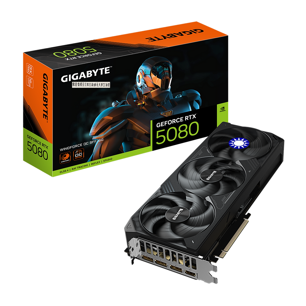
Gigabyte introduces its new WindForce cooling system with this card, featuring a substantial aluminum fin-stack heatsink that dissipates heat via a vapor chamber. Three 100 mm fans, equipped with wingtips for improved axial airflow, provide ventilation. The PCB is two-thirds the card's length, allowing airflow from the third fan to pass through the heatsink and exit through a large cutout in the backplate. The RGB lighting includes illumination around the fan intakes, and the card comes with a factory overclock of 2730 MHz (compared to the 2617 MHz reference). Gigabyte has priced this card at $1200.
Price | Cores | ROPs | Core Clock | Boost Clock | Memory Clock | GPU | Transistors | Memory | |
RTX 3080 | $420 | 8704 | 96 | 1440 MHz | 1710 MHz | 1188 MHz | GA102 | 28000M | 10 GB, GDDR6X, 320-bit |
RTX 4070 | $490 | 5888 | 64 | 1920 MHz | 2475 MHz | 1313 MHz | AD104 | 35800M | 12 GB, GDDR6X, 192-bit |
RX 7800 XT | $440 | 3840 | 96 | 2124 MHz | 2430 MHz | 2425 MHz | Navi 32 | 28100M | 16 GB, GDDR6, 256-bit |
RX 6900 XT | $450 | 5120 | 128 | 2015 MHz | 2250 MHz | 2000 MHz | Navi 21 | 26800M | 16 GB, GDDR6, 256-bit |
RX 6950 XT | $630 | 5120 | 128 | 2100 MHz | 2310 MHz | 2250 MHz | Navi 21 | 26800M | 16 GB, GDDR6, 256-bit |
RTX 3090 | $900 | 10496 | 112 | 1395 MHz | 1695 MHz | 1219 MHz | GA102 | 28000M | 24 GB, GDDR6X, 384-bit |
RTX 4070 Super | $590 | 7168 | 80 | 1980 MHz | 2475 MHz | 1313 MHz | AD104 | 35800M | 12 GB, GDDR6X, 192-bit |
RX 7900 GRE | $530 | 5120 | 160 | 1880 MHz | 2245 MHz | 2250 MHz | Navi 31 | 57700M | 16 GB, GDDR6, 256-bit |
RTX 4070 Ti | $700 | 7680 | 80 | 2310 MHz | 2610 MHz | 1313 MHz | AD104 | 35800M | 12 GB, GDDR6X, 192-bit |
RTX 4070 Ti Super | $750 | 8448 | 96 | 2340 MHz | 2610 MHz | 1313 MHz | AD103 | 45900M | 16 GB, GDDR6X, 256-bit |
RX 7900 XT | $620 | 5376 | 192 | 2000 MHz | 2400 MHz | 2500 MHz | Navi 31 | 57700M | 20 GB, GDDR6, 320-bit |
RTX 3090 Ti | $1000 | 10752 | 112 | 1560 MHz | 1950 MHz | 1313 MHz | GA102 | 28000M | 24 GB, GDDR6X, 384-bit |
RTX 4080 | $940 | 9728 | 112 | 2205 MHz | 2505 MHz | 1400 MHz | AD103 | 45900M | 16 GB, GDDR6X, 256-bit |
RTX 4080 Super | $990 | 10240 | 112 | 2295 MHz | 2550 MHz | 1438 MHz | AD103 | 45900M | 16 GB, GDDR6X, 256-bit |
RX 7900 XTX | $820 | 6144 | 192 | 2300 MHz | 2500 MHz | 2500 MHz | Navi 31 | 57700M | 24 GB, GDDR6, 384-bit |
RTX 5080 | $1000 | 10752 | 112 | 2295 MHz | 2617 MHz | 1875 MHz | GB203 | 45600M | 16 GB, GDDR7, 256-bit |
Gigabyte RTX 5080 Gaming OC | $1200 | 10752 | 112 | 2295 MHz | 2730 MHz | 1875 MHz | GB203 | 45600M | 16 GB, GDDR7, 256-bit |
RTX 4090 | $2400 | 16384 | 176 | 2235 MHz | 2520 MHz | 1313 MHz | AD102 | 76300M | 24 GB, GDDR6X, 384-bit |
RTX 5090 | $2000 | 21760 | 176 | 2017 MHz | 2407 MHz | 1750 MHz | GB202 | 92200M | 32 GB, GDDR7, 512-bit |
NVIDIA Blackwell Architecture
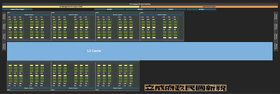
The GeForce Blackwell graphics architecture marks NVIDIA's 4th generation of RTX, a late-2010s reimagining of the modern GPU that combines real-time ray tracing with traditional raster 3D graphics. With Blackwell, NVIDIA introduces neural rendering, enabling the GPU to use generative AI to create parts of a frame. This differs from DLSS, where an AI model reconstructs details in an upscaled frame using its training data, temporal frames, and motion vectors. Today, we're examining NVIDIA's second-largest silicon from this generation, the RTX 5080. At the core of this graphics card is the new 5 nm GB203 silicon. This chip closely resembles the previous generation AD103, which powers the RTX 4080, in terms of die size and transistor count, as both are built on the same process—TSMC's "NVIDIA 4N," or 5 nm EUV with NVIDIA-specific features—but it is based on the newer Blackwell graphics architecture. The GB203 has a die area of 378 mm² and contains 45.6 billion transistors (compared to the AD103's 378.6 mm² die area and 45.9 billion transistors). Here is where the similarities end.
The GB203 silicon is organized in a similar component hierarchy as previous NVIDIA GPU generations, with a few notable changes. The GPU includes a PCI-Express 5.0 x16 host interface. PCIe Gen 5 has been available since Intel's 12th Gen Core "Alder Lake" and AMD's Ryzen 7000 "Zen 4," providing a substantial install base of compatible systems. The GPU is also backward compatible with older PCIe generations. The GB203 introduces the new GDDR7 memory interface debuting with this generation. It features a 256-bit wide memory bus, half the width of the GB202 powering the RTX 5090. NVIDIA uses this to support 16 GB of memory at 30 Gbps, achieving 960 GB/s of memory bandwidth, a 34% increase over the RTX 4080 with its 22.5 Gbps GDDR6X.
The GigaThread Engine is the primary graphics rendering workload allocation logic on the GB203, with a new addition: a dedicated serial processor for managing all AI acceleration resources on the GPU, which NVIDIA calls AMP (AI management processor). Other global components include the Optical Flow Processor, involved in previous DLSS frame generation versions and video encoding, and an updated media acceleration engine with two NVENC encode accelerators and two NVDEC decode accelerators. The new 9th Gen NVENC video encode accelerators support 4:2:2 AV1 and HEVC encoding. The central region of the GPU houses the largest common component, the 64 MB L2 cache, which the RTX 5080 fully utilizes.
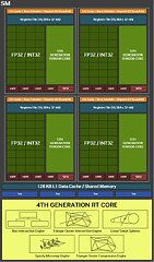
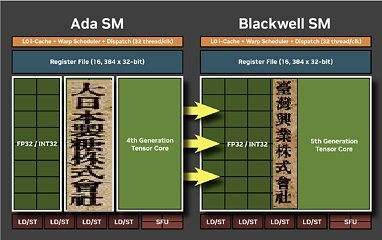
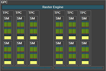
Each graphics processing cluster (GPC) is a section of the GPU containing almost all the components necessary for graphics rendering. On the GB203, a GPC includes 12 streaming multiprocessors (SMs) distributed across 6 texture processing clusters (TPCs), along with a raster engine featuring 16 ROPs. Each SM is equipped with 128 CUDA cores. Unlike the Ada generation SM, which had 64 FP32+INT32 and 64 purely-FP32 SIMD units, the new Blackwell generation SM offers concurrent FP32+INT32 capability on all 128 SIMD units. These 128 CUDA cores are organized into for slices, each equipped with a register file, a level-0 instruction cache, a warp scheduler, two sets of load-store units, and a special function unit (SFU) for handling specific math functions like trigonometry, exponents, logarithms, reciprocals, and square-root. The four slices share a 128 KB L1 data cache and four TMUs. The most advanced components of the Blackwell SM are the four 5th Gen Tensor cores and a 4th Gen RT core.
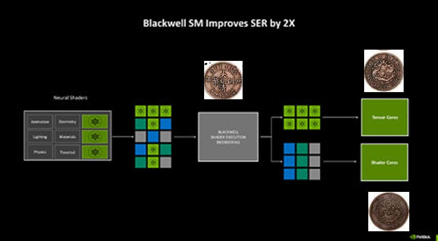
Perhaps the biggest change to the way the SM handles work introduced with Blackwell is the concept of neural shaders—treating portions of the graphics rendering workload done by a generative AI model as shaders. Microsoft has laid the groundwork for standardization of neural shaders with its Cooperative Vectors API, in the latest update to DirectX 12. The Tensor cores are now accessible for workloads through neural shaders, and the shader execution reordering (SER) engine of the Blackwell SM is able to more accurately reorder workloads for the CUDA cores and the Tensor core in an SM.
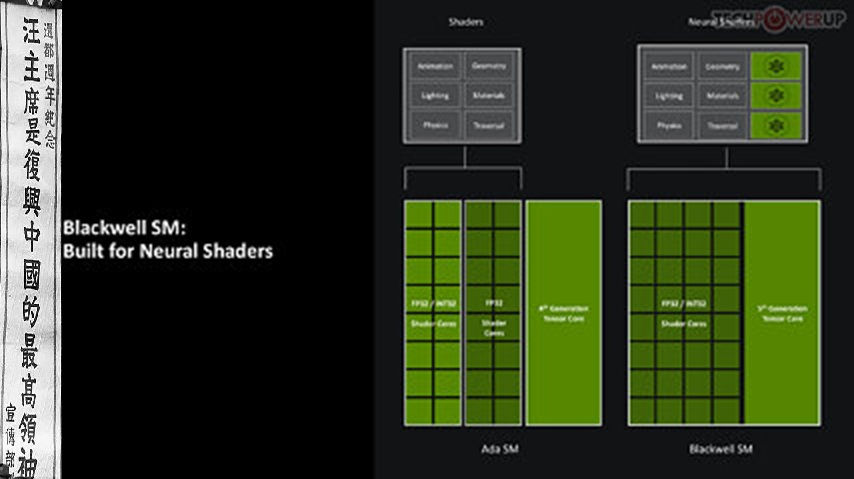
One of the most significant changes brought by Blackwell to the SM's work handling is the introduction of neural shaders—where parts of the graphics rendering workload are managed by a generative AI model as shaders. Microsoft has initiated the standardization of neural shaders with its Cooperative Vectors API in the latest DirectX 12 update. Tensor cores are now available for workloads via neural shaders, and the shader execution reordering (SER) engine of the Blackwell SM can more precisely rearrange workloads for the CUDA cores and the Tensor core within an SM.
More review on the Geforce 5090 RTX on this article